Metalenz, a Cambridge, Massachusetts company, announced a partnership with United Microelectronics Corporation (NYSE: UMC) for high-volume manufacturing of optical lenses using commercial semiconductor processing platforms. UMC, based in Taiwan, is amongst the largest semiconductor foundries in the world (after TSMC and Samsung) with a capitalization of ~$20B and annual revenues of ~$9B. The partnership enables high-volume manufacturing of optical lenses for 3D imaging in applications ranging from smartphones and laptops to IoT (Internet of Things) and automotive sensing.
The company was founded in 2017 as a spin-off from Federico Capasso’s group at Harvard University and focused on commercializing foundational IP (Intellectual Property) for metasurface-based passive optical elements like lenses. Professor Capasso has made seminal contributions in quantum cascade lasers, nanophotonics and metasurfaces and co-founded Metalenz, along with current CEO Rob Devlin.
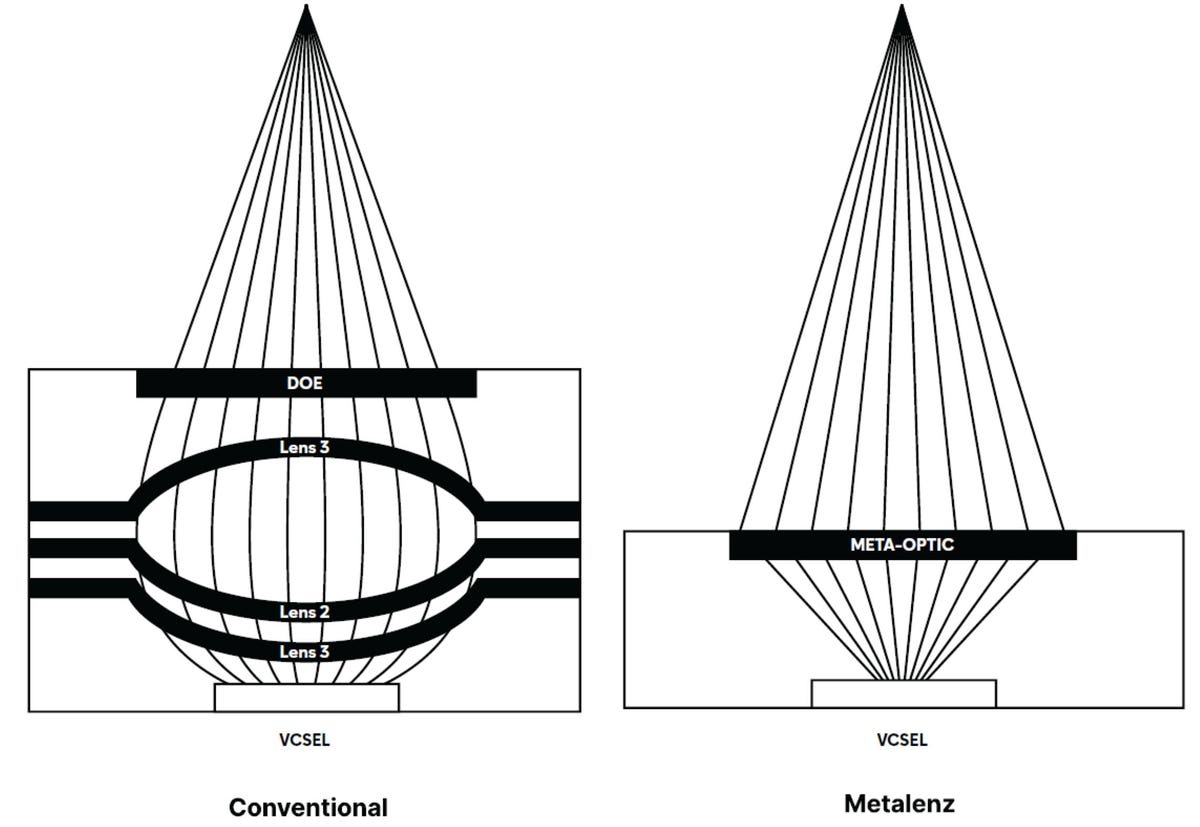
Traditional optical lenses of plastic or glass are composed of multiple curved surfaces since off-axis light must be bent to focus it. Meta-optics lenses work in a fundamentally different way. Nanoscale structures etched in silicon perform the bending function, with larger diameter structures slowing down the light (and, in effect creating the bend). Smaller diameter structures allow the light to pass through with reduced or no bending (see Figure 1).
A typical meta-optic lens for 3D imaging can have close to 10 million such structures laid out to create the appropriate light-focusing function. Instead of a bulky assembly composed of multiple layers, meta-optics technology enables flat lenses with significant performance, size and weight advantages. Such lenses are 100X thinner than conventional lenses, leading to ~50% more compact optical assemblies, a critical consideration for styling and integration in 3D imaging applications like smartphones and automotive sensing. Aberration losses are eliminated, leading to superior transmission performance, collection efficiency and beam quality for active imaging applications like LiDAR, which operate in narrow spectral windows (10-20 nm). Initial applications are targeted toward the Near Infrared (NIR) wavelengths (800-900 nm), although operation in other wavelength ranges is also possible.
Cost and integration ease are other significant advantages. Meta-optics lenses are fabricated in silicon and compatible with high-volume semiconductor foundry processes. Fabrication of the lenses requires a single mask and one-step lithography, with wafer-scale testing of individual lenses. Cumulative yields are much higher (fewer process steps). Chip-scale integration of such lenses with laser and detector chips becomes possible without complex packaging steps. This results in cost points at parity with plastic lenses (which have lower performance) and lower than glass lenses. As opposed to plastic lenses, meta-optic lenses can survive wider temperature ranges without performance degradation.
Metalenz announced a collaboration with ST Micro in 2022 to incorporate its flat lens technology into ST’s existing FlightSense ToF modules that serve applications such as smartphones, drones, robots, and vehicles. The company raised a $30M Series B funding round in late 2022. Investors include Neotribe Ventures, Intel Capital, Applied Materials, 3M and others. The funding is being deployed for floor space, staff expansion, and creating manufacturing partnerships with large commercial semiconductor foundries like UMC. Such partnerships are essential as OEMs increasingly use 3D sensing technology in high-volume consumer applications (smartphones and computers), IoT, security, automotive safety and autonomy. Development of this new supply chain allows Metalenz to service these large OEMs directly through the design-validation-manufacturing-supply cycle, assuring efficiency, quality and cost savings. Rob Devlin, founder and CEO: “As a fabless company, partnering with a leading semiconductor foundry like UMC gives Metalenz the performance and scale needed to satisfy the largest, most demanding customers in the consumer electronics industry. Launching our product in a major semiconductor foundry marks a fundamental change in the optics and semiconductor industry. By moving optics into the same foundry that produces electronics and sensors for the first time, Metalenz can now proliferate more advanced forms of sensing to billions of consumer devices and reshape the entire camera module supply chain.”
The initial designs for the newly established supply chain will be for a Chinese OEM, DiluSense, which supplies 3D sensing systems for IoT devices. Meta-optic lenses built on 300 mm diameter wafers have been qualified and start shipping in early July 2023. Dilusens’ products using these will ship in August 2023.
Read the full article here


